
I’m amazed no one has done this before, and there’s only one company doing it now. Microfabrica, based in Van Nuys, California, has perfected the technique of mass producing mechanical devices using the same electrodeposition technology used to make computer chips.
“We are the only high-volume production additive manufacturing platform in the market,” Microfabrica CEO Eric Miller tells me. “We use engineering grade metals to make commercially robust parts, and we’re focused on another end of the spectrum from where a lot of the 3D companies are focused, and that’s at the micro scale.”
The resulting devices are vanishingly small, and exquisitely made. How small? The company makes biopsy forceps less than a millimeter in diameter for a medical device company and timing mechanisms (i.e., clocks) that are less than half a centimeter across for a defense contractor, as well many other very small devices and precision parts.
The company’s manufacturing process builds up the parts from microns-thin layers of metal alloys on 4-inch or 6-inch ceramic wafers. Once the parts or devices are completed, technicians harvest them from the wafers—hundreds or tens of thousands of devices per wafer—and ship them off to customers in packaging designed for each type of device. Sometimes they pack them in vials of alcohol. Each part or device costs $1 to $100, depending on its complexity and how large it is (bigger parts cost more because they take up more space on the wafer).
Says Miller, “We’re the only ones who’ve been able to synthesize 3D printing with semiconductor manufacturing. That’s really the heart and soul of what we do. It’s what we call 3D printing, semiconductor style.”
I didn’t just take the company’s word for it. I asked a few experts from academia to weigh in on these claims, and they backed them up, albeit in typically cautious, understated fashion for folks who don’t want to be seen as endorsing products.
Here’s Jack Beuth, professor of mechanical engineering and director of the NextManufacturing Center at Carnegie Mellon University:
Microfabrica is filling a niche in providing very small scale metal 3d printing capability. The most popular 3d printing processes based on selective laser sintering (SLS) can produce features that are on the order of 200 microns (1/5 of a millimeter). “Micro” versions of SLS can produce features that are on the order of 70 to 100 microns in size (and the shapes produced at this size scale are not precisely dimensioned). The microfabrica process is clearly working with a greater level of precision.
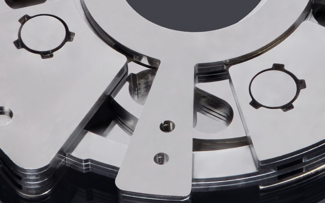
Here’s a graphic depiction of that “greater level of precision.”

On the left is a part made using Microfabrica’s process. On the right is a part made with the more conventional sintering process mentioned by Beuth. Also, as Miller points out, sintering is limited to prototyping and manufacturing in very small batches. Miller says 90% of his company’s revenue comes from high volume production.
The privately held company has been profitable for a couple of years now, and has stood up its own R&D lab for medical devices. The tiny revolution is just beginning.

Fascinating.